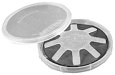
Sapphire Wafer Technology
High-quality sapphire wafers for advanced semiconductor and optical applications
Introduction to Sapphire Wafers
Sapphire (Al2O3) wafers are highly versatile substrates widely used in the semiconductor, optoelectronic, and LED industries. Known for their exceptional durability, high thermal conductivity, and optical transparency, sapphire wafers serve as an ideal foundation for various advanced technological applications.

At University Wafer, we provide high-quality sapphire wafers in various specifications to meet your research and production needs.
Single-Side vs. Double-Side Polished Sapphire Wafers
Single-Side Polished (SSP) Sapphire Wafers
Single-side polished sapphire wafers have one surface polished to a mirror-like finish while the other side remains unpolished or has a rougher finish.
Applications of SSP Sapphire Wafers:
- LED manufacturing
- Radio frequency integrated circuits (RFICs)
- Microelectromechanical systems (MEMS)
- Surface acoustic wave (SAW) devices
- Optical windows in high-pressure environments
Double-Side Polished (DSP) Sapphire Wafers
Double-side polished sapphire wafers have both surfaces polished to optical-grade finishes, offering superior optical properties and performance.
Applications of DSP Sapphire Wafers:
- High-precision optical components
- Infrared detectors
- Optical sensors
- Semiconductor on insulator (SOI) applications
- Transparent electronics
- Photonics applications requiring light transmission
Find a wide selection of both SSP and DSP sapphire wafers at University Wafer.
Sapphire Crystal Planes and Their Applications
Sapphire is an anisotropic crystal, meaning its properties vary depending on the crystallographic orientation. Different crystal planes offer unique properties suitable for specific applications.
C-plane (0001)
The most common orientation used for LED applications. Offers good thermal conductivity and is the standard for GaN epitaxy.
Applications: Blue and white LEDs, GaN power devices
A-plane (11-20)
Provides reduced polarization effects and improved internal quantum efficiency for LED applications.
Applications: Non-polar GaN growth, high-performance LEDs
R-plane (1-102)
Offers excellent lattice matching with silicon for SOS (Silicon-on-Sapphire) technology.
Applications: SOS devices, RF circuits, radiation-hardened electronics
M-plane (10-10)
Another non-polar plane that enables improved efficiency in gallium nitride-based devices.
Applications: High-efficiency LEDs, semiconductor lasers
Browse our full range of sapphire wafers with various crystal orientations to find the perfect match for your application.
Indium Tin Oxide (ITO) Deposition on Sapphire Wafers
Indium Tin Oxide (ITO) is a transparent conducting oxide commonly deposited on sapphire wafers to create transparent electrodes for various applications.
ITO Deposition Methods
| Deposition Method | Description | Advantages |
|---|---|---|
| RF Magnetron Sputtering | Uses radio frequency power to create plasma that deposits ITO onto the sapphire substrate | High-quality films, excellent uniformity, good adhesion |
| DC Sputtering | Direct current-based sputtering method for ITO deposition | High deposition rates, cost-effective, suitable for large areas |
| Eletron Beacm Evaporation | Uses an electron beam to evaporate ITO material in a vacuum chamber | Precise thickness control, high purity films |
| Pulsed Laser Deposition (PLD) | Uses laser pulses to vaporize ITO from a target onto the sapphire substrate | Excellent stoichiometry control, high-quality epitaxial films |
Applications of ITO-Coated Sapphire Wafers
- Transparent electrodes for optoelectronic devices
- LCD displays and touchscreens
- Organic light-emitting diodes (OLEDs)
- Solar cells
- Electrochromic windows
- Infrared reflectors
- Anti-static coatings
- EMI shielding with optical transparency
The combination of sapphire's excellent optical properties and ITO's electrical conductivity makes ITO-coated sapphire wafers ideal for applications requiring both transparency and conductivity.
Contact University Wafer for custom ITO-coated sapphire wafers or explore our range of pre-coated options.
Why Choose Our Sapphire Wafers?
- High-quality crystal growth with minimal defects
- Precise dimensional control and tight tolerances
- Multiple crystal orientations available
- Custom sizes and specifications
- Expert technical support
- Quick turnaround times
- Competitive pricing for both research and production quantities
Ready to order? Browse our selection of sapphire wafers or contact our team for custom requirements.